
ファイル:Cmos-chip structure in 2000s (en).svg

この SVG ファイルのこの PNG プレビューのサイズ: 407 × 599 ピクセル. その他の解像度: 163 × 240 ピクセル | 326 × 480 ピクセル | 521 × 768 ピクセル | 695 × 1,024 ピクセル | 1,390 × 2,048 ピクセル | 550 × 810 ピクセル。
元のファイル (SVG ファイル、550 × 810 ピクセル、ファイルサイズ: 138キロバイト)
ウィキメディア・コモンズのファイルページにある説明を、以下に表示します。
|
概要
| 解説 |
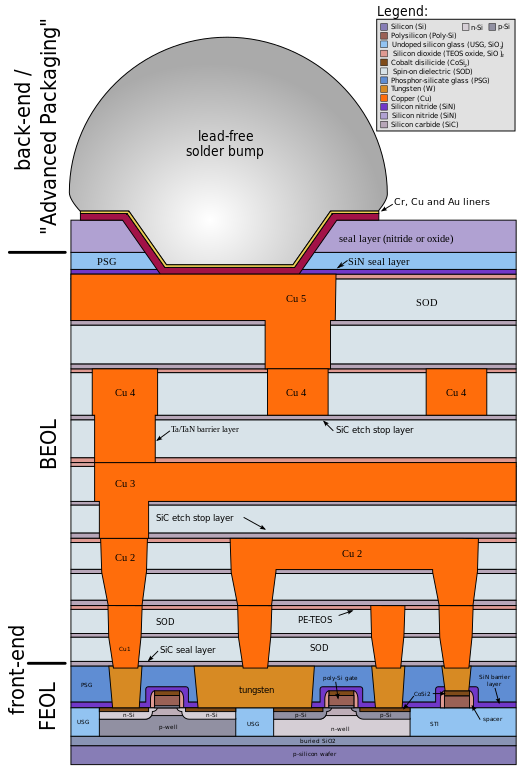
Català: Estructura esquemàtica d'un xip CMOS, tal com es va construir a principis dels anys 2000. El gràfic mostra els LDD-MISFET sobre un substrat de silici SOI amb cinc capes de metal·lització i un tap de soldadura per a la unió de xip. També mostra la secció per a FEOL (front-end de línia), BEOL (back-end de línia) i les primeres parts del procés de back-end. (versió traduïda a l'alemany)
English: Schematic structure of a CMOS chip, like it is built in the early 2000s. The graphic shows LDD-MISFET's on a SOI silicon substrate with five metallization layers and solder bump for flip-chip bonding. Also it shows the section for FEOL (front-end of line), BEOL (back-end of line) and first parts of back-end process. (translated German version) |
| 日付 | 2006年12月9日 (アップロード日) |
| 原典 | self made (from university scripts and scientific papers) |
| 作者 | Cepheiden |
| その他のバージョン |
Other related versions:[]
|
.svg&lang=ca)
.svg&lang=en)

.svg)
.svg?uselang=ja)
.svg?uselang=ja)
.svg?uselang=ja&action=history)
.svg)
.svg)
|
このSVGファイルには翻訳可能な埋め込みテキストが含まれています。SVG翻訳ツールや他のSVGエディタを使用して自分の言語に翻訳可能です。詳しくはSVGファイルの翻訳についてを参照してください。 |
.svg)
このファイルはSVGの 翻訳済みであるあなたの言語でこのファイルを利用するときは、言語コードと また、このファイルをあなたの言語に翻訳するには、ファイルをダウンロードし、翻訳を追加して、このファイルと同じ名前で再アップロードして下さい。不明瞭な点がある場合は Graphics Lab が役に立つでしょう。 |
ライセンス
この作品の著作権者である私は、この作品を以下のライセンスで提供します。

|
この文書は、フリーソフトウェア財団発行のGNUフリー文書利用許諾書 (GNU Free Documentation License) 1.2またはそれ以降のバージョンの規約に基づき、複製や再配布、改変が許可されます。不可変更部分、表紙、背表紙はありません。このライセンスの複製は、GNUフリー文書利用許諾書という章に含まれています。 |
| このファイルはクリエイティブ・コモンズ 表示-継承 3.0 非移植ライセンスのもとに利用を許諾されています。 | ||
| ||
| このライセンスのテンプレートは、GFDLのライセンス・アップデートによりこのファイルに追加されたものです。 |
このファイルはクリエイティブ・コモンズ 表示 2.5 一般ライセンスのもとに利用を許諾されています。
- あなたは以下の条件に従う場合に限り、自由に
- 共有 – 本作品を複製、頒布、展示、実演できます。
- 再構成 – 二次的著作物を作成できます。
- あなたの従うべき条件は以下の通りです。
- 表示 – あなたは適切なクレジットを表示し、ライセンスへのリンクを提供し、変更があったらその旨を示さなければなりません。これらは合理的であればどのような方法で行っても構いませんが、許諾者があなたやあなたの利用行為を支持していると示唆するような方法は除きます。
あなたは上記のライセンスから、どれか一つ以上を選択できます。
ファイルの履歴
過去の版のファイルを表示するには、その版の日時をクリックしてください。
| 日付と時刻 | サムネイル | 寸法 | 利用者 | コメント | |
|---|---|---|---|---|---|
| 現在の版 | 2024年2月5日 (月) 14:35 | | 550 × 810 (138キロバイト) | Manlleus | File uploaded using svgtranslate tool (https://svgtranslate.toolforge.org/). Added translation for ca. |
| 2024年2月5日 (月) 14:25 |  | 550 × 810 (97キロバイト) | Manlleus | fixed text labels for translation | |
| 2006年12月9日 (土) 18:52 |  | 550 × 810 (85キロバイト) | Cepheiden | {{Information |Description= Schematic structure of a CMOS chip, like it is build in the early 2000s. The grafic shows LDD-MISFET's on a SOI silicon substrate with five metallization layers and solder bump for flip-chip bonding. Also it shows the section f | |
| 2006年12月9日 (土) 18:49 |  | 550 × 810 (85キロバイト) | Cepheiden | {{Information |Description= Schematic structure of a CMOS chip, like it is build in the early 2000s. The grafic shows LDD-MISFET's on a SOI silicon substrate with five metallization layers and solder bumb for flip-chip bonding. Also it shows the section f |
ファイルの使用状況
グローバルなファイル使用状況
以下に挙げる他のウィキがこの画像を使っています:
- ar.wikipedia.org での使用状況
- ca.wikipedia.org での使用状況
- en-two.iwiki.icu での使用状況
- fa.wikipedia.org での使用状況
- fi.wikipedia.org での使用状況
- hy.wikipedia.org での使用状況
- id.wikipedia.org での使用状況
- ko.wikipedia.org での使用状況
- zh-two.iwiki.icu での使用状況
.svg)