利用者:加藤勝憲/トライアック
 A small plastic-cased TRIAC device mounted on a printed circuit board
| |
| Type | Active |
|---|---|
| Pin configuration | Terminal1, gate and Terminal2 |
| Electronic symbol | |

| |
トライアック(TRIAC、triode for alternating current)はは、トリガをかけると、どちらかの方向に電流を流せる3端子の電子部品である。TRIACという用語は商標が普通名称化したものである。 bidirectional triode thyristorまたはbilateral triode thyristor[1]とも呼ばれる。
TRIACはサイリスタ(小さな電圧と電流ではるかに大きな電圧と電流を制御できるという点でリレーに類似)のサブセットであり、シリコン制御整流器(SCR)に関連している。TRIACがSCRと異なる点は、SCRが一方向にしか電流を流せないのに対し、TRIACは両方向に電流を流すことができる点である。ほとんどのTRIACは、ゲートに正または負の電圧を印加することでトリガーできる(SCRは正の電圧を必要とする)。いったんトリガーされると、SCRとTRIACは、ゲート電流が停止しても、主電流が保持電流と呼ばれる一定レベル以下に低下するまで導通し続ける。
ゲートターンオフサイリスタ(Gate turn-off thyristor
、GTO)はTRIACに似ているが、ゲート信号が停止したときにオフになることで、より高い制御性を提供する。
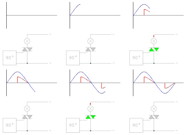
TRIACの双方向性により、交流(AC)用のスイッチとして便利です。さらに、主回路の交流の制御された位相角でトリガーを印加することにより、負荷に流れる平均電流を制御することができる(位相制御)。これは、ユニバーサル・モーターの速度制御、ランプの調光、電気ヒーターの制御などによく使用される。TRIACはバイポーラ・デバイスである。
The bidirectionality of TRIACs makes them convenient switches for alternating-current (AC). In addition, applying a trigger at a controlled phase angle of the AC in the main circuit allows control of the average current flowing into a load (phase control). This is commonly used for controlling the speed of a universal motor, dimming lamps, and controlling electric heaters. TRIACs are Bipolar devices.
Operation
[編集]
TRIACの動作を理解するために、MT1に対するゲート電圧とMT2電圧の4つの可能な組み合わせのそれぞれにおけるトリガーを考える。4つの個別のケース(象限)を図 1 に示す。主端子 1(MT1)と主端子(MT2)は、それぞれアノード 1(A1)、アノード 2(A2)とも呼ばれる[2]。
相対的な感度は特定のトライアックの物理的構造に依存するが、原則として、第 I 象限が最も感度が高く(必要なゲート電流が最も少ない)、第 4 象限が最も感度が低い(必要なゲート電流が最も多い)[clarification needed なぜ Q-IV が最も感度が低いのか? 議論を参照]。
The relative sensitivity depends on the physical structure of a particular triac, but as a rule, quadrant I is the most sensitive (least gate current required), and quadrant 4 is the least sensitive (most gate current required).[要説明][<span title="The text near this tag may need clarification or removal of jargon. (October 2011)">clarification needed</span> Why is Q-IV the least sensitive? See discussion]
第1象限と第2象限では、MT2が正で、電流はMT2からP、N、P、N層を通ってMT1に流れる。MT2に接続されたN領域は大きく関与しない。第3象限と第4象限では、MT2は負で、電流はMT1からMT2へ、やはりP、N、P、N層を通って流れる。MT2に付着したN領域は活性であるが、MT1に付着したN領域は最初のトリガーに関与するだけで、バルク電流の流れには関与しない。
ほとんどのアプリケーションでは、ゲート電流はMT2から供給されるため、第1象限と第3象限が唯一の動作モードとなる(ゲートとMT2の両方がMT1に対して正または負)。IC やデジタル駆動回路からの単一極性トリガを使用する他のアプリケーションでは、MT1 が通常正電圧(例:+5V など)に接続され、ゲートが 0V(グランド)にプルダウンされる第 2 および第 3 クワドラントで動作する。
Quadrant 1
[編集]
第1象限動作は、ゲートとMT2がMT1に対して正であるときに発生する。
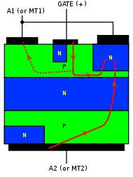
Quadrant 1 operation occurs when the gate and MT2 are positive with respect to MT1.Figure 1
そのメカニズムを図3に示す。ゲート電流は同等のNPNトランジスタをオンにし、そのNPNトランジスタは同等のPNPトランジスタのベースから電流を引き出して、これもオンにする。ゲート電流の一部(点線)は、p-シリコンを横切るオーミック経路を通して失われ、NPNトランジスタのベースを通らずにMT1に直接流れ込む。この場合、pシリコンに正孔が注入されることで、MT1の下に積層されたn、p、n層がNPNトランジスタのように動作し、ベースに電流が存在するためにオンになる。これにより、MT2の上のp、n、p層はPNPトランジスタのように動作し、そのn型ベースがエミッタ(MT2)に対して順バイアスになるためオンする。従って、トリガー方式はSCRと同じである。等価回路を図4に示す。
そのメカニズムを図3に示す。ゲート電流は同等のNPNトランジスタをオンにし、そのNPNトランジスタは同等のPNPトランジスタのベースから電流を引き出して、これもオンにする。ゲート電流の一部(点線)は、p-シリコンを横切るオーミック経路を通して失われ、NPNトランジスタのベースを通らずにMT1に直接流れ込む。この場合、pシリコンに正孔が注入されることで、MT1の下に積層されたn、p、n層がNPNトランジスタのように動作し、ベースに電流が存在するためにオンになる。これにより、MT2の上のp、n、p層はPNPトランジスタのように動作し、そのn型ベースがエミッタ(MT2)に対して順バイアスになるためオンする。従って、トリガー方式はSCRと同じである。等価回路を図4に示す。
一般に、この象限は 4 つの象限の中で最も高感度である。これは、ゲート電流がメイン・デバイス・トランジスタの1つのベースに直接注入される唯一の象限だからである[2]。
Quadrant 2
[編集]
クワドラント2の動作は、ゲートが負でMT2がMT1に対して正である場合に発生する。
Quadrant 2 operation occurs when the gate is negative and MT2 is positive with respect to MT1.Figure 1
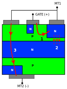
図 5 にトリガー・プロセスを示す。デバイスのターンオンは3重構造になっており、MT1からの電流がゲート下のp-n接合を介してゲートに流れ込むことで開始する。これにより、ゲートをカソードとするNPNトランジスタとPNPトランジスタで構成される構造がスイッチオンする(この構造のターンオンは図中 "1 "で示されている)。ゲートへの電流が増加すると、ゲートとMT2間の電位差が低下する傾向にあるため、ゲート下のp-シリコンの左側の電位がMT1に向かって上昇します。これにより、p-シリコンの左側と右側の間に電流が流れ(図では「2」で示される)、MT1端子下のNPNトランジスタがオンになり、その結果、MT2とp-シリコンの上側の右側の間のpnpトランジスタもオンになります。つまり、結局、電流の主要部分が横切る構造は、クワドラントI動作(図5の「3」)と同じである[3]。
Quadrant 3
[編集]
クワドラント3の動作は、ゲートとMT2がMT1に対して負であるときに発生する。
Quadrant 3 operation occurs when the gate and MT2 are negative with respect to MT1.Figure 1
プロセス全体の概略は図6に示されている。ここでもプロセスは異なるステップで起こる。最初の段階では、MT1端子とゲート間のpn接合が順バイアスになる(ステップ1)。順バイアスは接合に加わる2つの層に少数キャリアが注入されることを意味するため、電子はゲート下のp層に注入される。これらの電子の一部は再結合せず、下層のn領域に逃げ込む(ステップ2)。これによりn領域の電位が下がり、pnpトランジスタのベースとして機能し、スイッチがオンになる(ベース電位を直接下げずにトランジスタをオンにすることをリモート・ゲート制御と呼ぶ)。下層のp層は、このPNPトランジスタのコレクターとして働き、その電圧を上昇させます。このp層はまた、すぐ上の最後の3層で構成されるNPNトランジスタのベースとしても働く。
Quadrant 4
[編集]
Quadrant 4 operation occurs when the gate is positive and MT2 is negative with respect to MT1. Figure 1
Triggering in this quadrant is similar to triggering in quadrant III. The process uses a remote gate control and is illustrated in Figure 7. As current flows from the p-layer under the gate into the n-layer under MT1, minority carriers in the form of free electrons are injected into the p-region and some of them are collected by the underlying n-p junction and pass into the adjoining n-region without recombining. As in the case of a triggering in quadrant III, this lowers the potential of the n-layer and turns on the PNP transistor formed by the n-layer and the two p-layers next to it. The lower p-layer works as the collector of this PNP transistor and has its voltage heightened: this p-layer also acts as the base of an NPN transistor made up by the last three layers just over the MT2 terminal, which, in turn, gets activated. Therefore, the red arrow labeled with a "3" in Figure 6 shows the final conduction path of the current.
Generally, this quadrant is the least sensitive of the four. In addition, some models of TRIACs (logic level and snubberless types) cannot be triggered in this quadrant but only in the other three.
Issues
[編集]There are some limitations one should know when using a TRIAC in a circuit. In this section, a few are summarized.
Gate threshold current, latching current and holding current
[編集]A TRIAC starts conducting when a current flowing into or out of its gate is sufficient to turn on the relevant junctions in the quadrant of operation. The minimum current able to do this is called gate threshold current and is generally indicated by IGT. In a typical TRIAC, the gate threshold current is generally a few milliamperes, but one has to take into account also that:
- IGT depends on the temperature: The higher the temperature, the higher the reverse currents in the blocked junctions. This implies the presence of more free carriers in the gate region, which lowers the gate current needed.
- IGT depends on the quadrant of operation, because a different quadrant implies a different way of triggering (see here). As a rule, the first quadrant is the most sensitive (i.e. requires the least current to turn on), whereas the fourth quadrant is the least sensitive.
- When turning on from the off state, IGT depends on the voltage across the two main terminals MT1 and MT2. Higher voltage between MT1 and MT2 cause greater reverse currents in the blocked junctions, thus requiring less gate current to trigger the device (similar to high temperature operation). In datasheets IGT is generally given for a specified voltage between MT1 and MT2.
When the gate current is discontinued, if the current between the two main terminals is more than what is called the latching current, the device continues to conduct. Latching current is the minimum current that keeps the device internal structure latched in the absence of gate current. The value of this parameter varies with:
- gate current pulse (amplitude, shape and width)
- temperature
- quadrant of operation
In particular, if the pulse width of the gate current is sufficiently large (generally some tens of microseconds), the TRIAC has completed the triggering process when the gate signal is discontinued and the latching current reaches a minimum level called holding current. Holding current is the minimum required current flowing between the two main terminals that keeps the device on after it has achieved commutation in every part of its internal structure.
In datasheets, the latching current is indicated as IL, while the holding current is indicated as IH. They are typically in the order of some milliamperes.
Static dv/dt
[編集]A high between MT2 and MT1 may turn on the TRIAC when it is off. Typical values of critical static dv/dt are in the terms of volts per microsecond.
The turn-on is due to a parasitic capacitive coupling of the gate terminal with the MT2 terminal, which lets currents into the gate in response to a large rate of voltage change at MT2. One way to cope with this limitation is to design a suitable RC or RCL snubber network. In many cases this is sufficient to lower the impedance of the gate towards MT1. By putting a resistor or a small capacitor (or both in parallel) between these two terminals, the capacitive current generated during the transient flows out of the device without activating it. A careful reading of the application notes provided by the manufacturer and testing of the particular device model to design the correct network is in order. Typical values for capacitors and resistors between the gate and MT1 may be up to 100 nF and 10 Ω to 1 kΩ. Normal TRIACs, except for low-power types marketed as sensitive gate,[3] already have such a resistor built in to safeguard against spurious dv/dt triggering. This will mask the gate's supposed diode-type behaviour when testing a TRIAC with a multimeter.
In datasheets, the static dv/dt is usually indicated as and, as mentioned before, is in relation to the tendency of a TRIAC to turn on from the off state after a large voltage rate of rise even without applying any current in the gate.
Critical di/dt
[編集]A high rate of rise of the current between MT1 and MT2 (in either direction) when the device is turning on can damage or destroy the TRIAC even if the pulse duration is very short. The reason is that during the commutation, the power dissipation is not uniformly distributed across the device. When switching on, the device starts to conduct current before the conduction finishes to spread across the entire junction. The device typically starts to conduct the current imposed by the external circuitry after some nanoseconds or microseconds but the complete switch on of the whole junction takes a much longer time, so too swift a current rise may cause local hot spots that can permanently damage the TRIAC.
In datasheets, this parameter is usually indicated as and is typically in the order of the tens of ampere per microsecond.
Commutating dv/dt and di/dt
[編集]The commutating dv/dt rating applies when a TRIAC has been conducting and attempts to turn off with a partially reactive load, such as an inductor. The current and voltage are out of phase, so when the current decreases below the holding value, the TRIAC attempts to turn off, but because of the phase shift between current and voltage, a sudden voltage step takes place between the two main terminals, which turns the device on again.
In datasheets, this parameter is usually indicated as and is generally in the order of up to some volts per microsecond.
The reason why commutating dv/dt is less than static dv/dt is that, shortly before the device tries to turn off, there is still some excess minority charge in its internal layers as a result of the previous conduction. When the TRIAC starts to turn off, these charges alter the internal potential of the region near the gate and MT1, so it is easier for the capacitive current due to dv/dt to turn on the device again.
Another important factor during a commutation from on-state to off-state is the di/dt of the current from MT1 to MT2. This is similar to the recovery in standard diodes: the higher the di/dt, the greater the reverse current. Because in the TRIAC there are parasitic resistances, a high reverse current in the p-n junctions inside it can provoke a voltage drop between the gate region and the MT1 region which may make the TRIAC stay turned on.
In a datasheet, the commutating di/dt is usually indicated as and is generally in the order of some amperes per microsecond.
The commutating dv/dt is very important when the TRIAC is used to drive a load with a phase shift between current and voltage, such as an inductive load. Suppose one wants to turn the inductor off: when the current goes to zero, if the gate is not fed, the TRIAC attempts to turn off, but this causes a step in the voltage across it due to the aforementioned phase shift. If the commutating dv/dt rating is exceeded, the device will not turn off.
Snubber circuits
[編集]When used to control reactive (inductive or capacitive) loads, care must be taken to ensure that the TRIAC turns off correctly at the end of each half-cycle of the AC in the main circuit. TRIACs can be sensitive to fast voltage changes (dv/dt) between MT1 and MT2, so a phase shift between current and voltage caused by reactive loads can lead to a voltage step that can turn the thyristor on erroneously. An electric motor is typically an inductive load and off-line power supplies—as used in most TVs and computers—are capacitive.
Unwanted turn-ons can be avoided by using a snubber circuit (usually of the resistor/capacitor or resistor/capacitor/inductor type) between MT1 and MT2. Snubber circuits are also used to prevent premature triggering, caused for example by voltage spikes in the mains supply.
Because turn-ons are caused by internal capacitive currents flowing into the gate as a consequence of a high dv/dt, (i.e., rapid voltage change) a gate resistor or capacitor (or both in parallel) may be connected between the gate and MT1 to provide a low-impedance path to MT1 and further prevent false triggering. This, however, increases the required trigger current or adds latency due to capacitor charging. On the other hand, a resistor between the gate and MT1 helps draw leakage currents out of the device, thus improving the performance of the TRIAC at high temperature, where the maximum allowed dv/dt is lower. Values of resistors less than 1kΩ and capacitors of 100nF are generally suitable for this purpose, although the fine-tuning should be done on the particular device model.
For higher-powered, more-demanding loads, two SCRs in inverse parallel may be used instead of one TRIAC. Because each SCR will have an entire half-cycle of reverse polarity voltage applied to it, turn-off of the SCRs is assured, no matter what the character of the load. However, due to the separate gates, proper triggering of the SCRs is more complex than triggering a TRIAC.
TRIACs may also fail to turn on reliably with reactive loads if the current phase shift causes the main circuit current to be below the holding current at trigger time. To overcome the problem DC or a pulse train may be used to repeatedly trigger the TRIAC until it turns on.
Application
[編集]
Low-power TRIACs are used in many applications such as light dimmers, speed controls for electric fans and other electric motors, and in the modern computerized control circuits of many household small and major appliances.
When mains voltage TRIACs are triggered by microcontrollers, optoisolators are frequently used; for example optotriacs can be used to control the gate current. Alternatively, where safety allows and electrical isolation of the controller isn't necessary, one of the microcontroller's power rails may be connected to one of the mains supply. In these situations it is normal to connect the neutral terminal to the positive rail of the microcontroller's power supply, together with A1 of the triac, with A2 connected to the live. The TRIAC's gate can be connected through an opto-isolated transistor, and sometimes a resistor to the microcontroller, so that bringing the voltage down to the microcontroller's logic zero pulls enough current through the TRIAC's gate to trigger it. This ensures that the TRIAC is triggered in quadrants II and III and avoids quadrant IV where TRIACs are typically insensitive.
Example data
[編集]| Variable name | Parameter | Typical value | Unit |
|---|---|---|---|
| Gate threshold voltage | 0.7–1.5 | V | |
| Gate threshold current | 5–50 | mA | |
| Repetitive peak off-state forward voltage | 600–800 | V | |
| Repetitive peak off-state reverse voltage | 600–800 | V | |
| RMS on-state current | 4–40 | A | |
| On-state current, non-repetitive peak | 100–270 | A | |
| On-state forward voltage | 1.5 | V |
High commutation (two- and three-quadrant) TRIACs
[編集]Three-quadrant TRIACs only operate in quadrants 1 through 3 and cannot be triggered in quadrant 4. These devices are made specifically for improved commutation and can often control reactive loads without the use of a snubber circuit.
The first TRIACs of this type were marketed by Thomson Semiconductors (now ST Microelectronics) under the name "Alternistor". Later versions are sold under the trademark "Snubberless" and "ACS" (AC Switch, though this type also incorporates a gate buffer, which further precludes Quadrant I operation). Littelfuse also uses the name "Alternistor". Philips Semiconductors (now NXP Semiconductors) originated the trademark "Hi-Com" (High Commutation).
Often these TRIACs can operate with smaller gate-current to be directly driven by logic level components.
関連項目
[編集]脚注・参考文献
[編集]- ^ Bhimsen (2020年10月6日). “Thyristor or Silicon Controlled Rectifier (SCR)” (英語). electronics fun. 2021年10月31日閲覧。
- ^ “TRIAC – Operation, symbol, circuits & applications”. Electrical Classroom (15 July 2021). Template:Cite webの呼び出しエラー:引数 accessdate は必須です。
- ^ “2N6071A/B Series Sensitive Gate Triacs”. Littelfuse. January 9, 2023閲覧。
- ^ “Philips Semiconductors Product specification Triacs BT138 series”. 2016年12月13日時点のオリジナルよりアーカイブ。2016年11月23日閲覧。 090119 nxp.com
- ^ “STMicroelectronics T3035H, T3050H Snubberless high temperature 30 A Triacs”. Template:Cite webの呼び出しエラー:引数 accessdate は必須です。 st.com 100922
引用エラー: <references> で定義されている name "ThyristorTheory" の <ref> タグは、先行するテキスト内で使用されていません。
引用エラー: <references> で定義されている name "PowerElec" の <ref> タグは、先行するテキスト内で使用されていません。
<references> で定義されている name "AN3008" の <ref> タグは、先行するテキスト内で使用されていません。関連文献
[編集]- Thyristor Theory and Design Considerations; ON Semiconductor; 240 pages; 2006; HBD855/D. (Free PDF download)
 ウィキメディア・コモンズには、加藤勝憲/トライアックに関するカテゴリがあります。
[[Category:パワーエレクトロニクス]] [[Category:未査読の翻訳があるページ]]


